Nanoparticle Enhanced Detecting Medium:
The detector platform being investigated dopes a scintillating resin with tailored nanoparticles specific to radiation species. The nanoparticles act as a conversion mechanism to create charged particles (fast electrons) when radiation interacts with the nanoparticles. WO3, Pb3O4, glass nanoparticles, and Gd2O3 are used for beta, gamma/X-ray, alpha, and neutron detectors, respectively (Fig. 1). Doping the resin with nanoparticles, the scintillator becomes more sensitive to the four species of ionizing radiation that are emitted from fissionable materials. Liberated electrons scintillate the matrix creating the characteristic light pulse which is allowed to exit the detector since the diameter of the nanoparticles is smaller than the wavelength of the created light. Gadolinium has the largest neutron absorption cross section of any material and converts thermal neutrons directly into fast electrons. The Gd/neutron reaction results in several products including gamma rays and conversion electrons. Since the detector head is thin, the produced gamma rays pass through the material with a lower probability of reacting with the scintillating resin making the fast electron the only useable product. The release of a fast electron occurs in 39% of the captured interactions with an electron energy of 72 keV, making the optical pulse detected extremely characteristic to a neutron interaction (Fig. 2). This characteristic pulse easily allows for pulse height spectroscopy for differentiating between neutron radiation and other detected species. The emitted light pulses are detected with a Photo-Multiplier (PM) tube which produces a measurable current from the created light pulses. The different nanoparticles used convert differing radiation species into electrons through independent physical mechanisms including charge conversion (alpha), secondary electron (beta), photoelectron (gamma/x-rays), and an on-chip thermonuclear fusion reaction (neutron) allowing for the detection and discrimination all four ionizing species on a single device (Fig. 3).
Interfacing Circuitry:
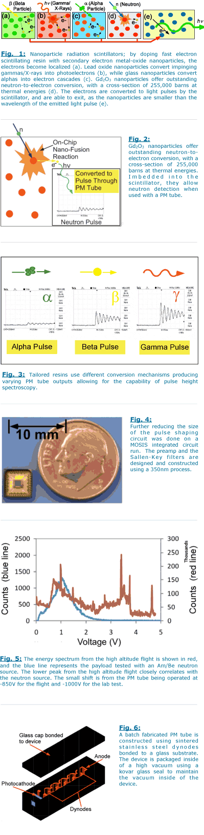
A completely packaged lightweight field radiation detector is essential for real world applications. The design of the circuit needs to preserve as much information as possible that was produced in the scintillator in order to discriminate and perform energy spectroscopy which is a vital capability for the previously discussed scintillators. This is needed to differentiate between weapons grade nuclear material and harmful biological isotopes. Current field detectors that are able to perform the above task are extremely bulky and expensive. The designed circuitry uses a charge sensitive preamplifier that integrates the current from the PM tube to represent the total charge deposited in the scintillator. The output of the preamplifier is further shaped by a two stage Sallen-Key filter that produces a Gaussian shaped pulse for easier peak acquisition. The pulse is converted to a digital signal and either stored on flash memory or transferred via wireless communication to a portable electronic device for interfacing with the user. The pulse shaping circuitry is designed and constructed on both a PC board and an integrated circuit for further size reduction (Fig. 4). Also, the power supply for the high voltage needed for the PM tube is being designed and fabricated in house for a >10 fold reduction in power consumption when compared with off the shelf converters. The overall design of the circuitry for the entire portable radiation detector should use less than 25 mA of current at a single supply voltage of 5 V which allowing for a longer battery life. A portable detector using a gadolinium loaded scintillator was previously tested separately in a near space environment and with an Am/Be neutron source. The lower peak of the detector is associated with neutron radiation releasing the characteristic 72 keV electron while the higher pulses are associated with higher energy gamma radiation (Fig. 5).
Miniaturized Batch Fabricated PM tube:
Currently off the shelf PM tubes are expensive and manufactured by hand. The basic components of a PM tube are a photocathode, series of dynodes, and an anode (Fig. 6). The proposed design uses a box and grid dynode layout due to the symmetric nature of the design making it easier to batch fabricate. The box grid type is the most common type of layout because of the overall performance of the design. The design uses a sintered stainless steel fabrication process because of the batch fabrication ability. A master mold is micromilled inside of a stock of Teflon. A disposable reverse mold is then fabricated with a two part urethane casting resin to create the final mold for the green stainless steel parts held together by a binding agent. After the dynodes are sintered, a thin secondary electron emission coating is applied to the surface using a metal deposition technique. The dynode pattern is placed on a glass substrate so the sintered stainless steel parts can be easily bonded to the surface in the correct location automatically. The cap is etched using a microbead blasting process to rapidly etch a cavity to house the dynodes. The photocathode material is deposited on the side of the etched cavity before the device is packaged. The bottom substrate containing the sintered dynodes and etched top glass are bonded inside of a vacuum chamber using a kovar glass seal.